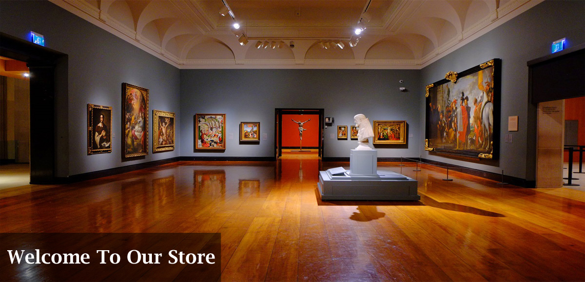
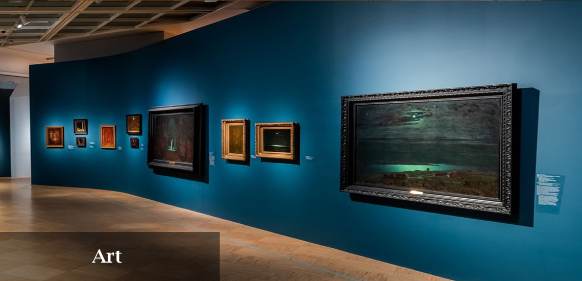
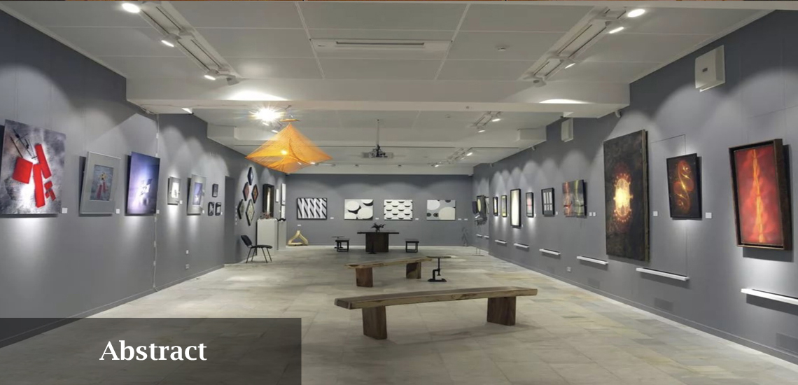
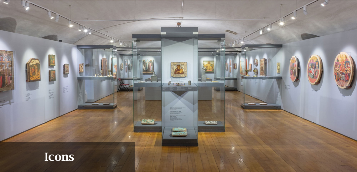
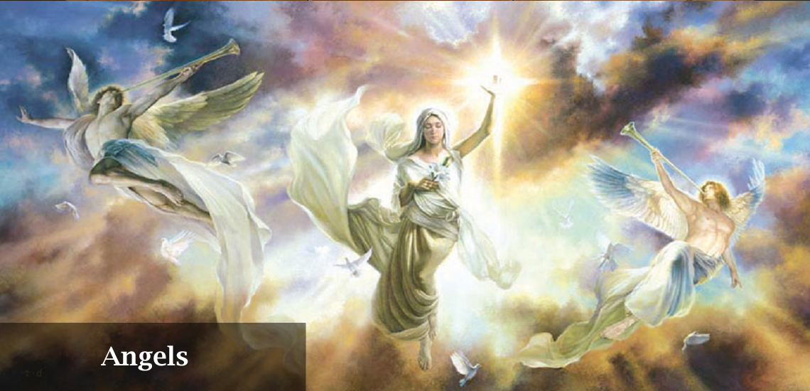
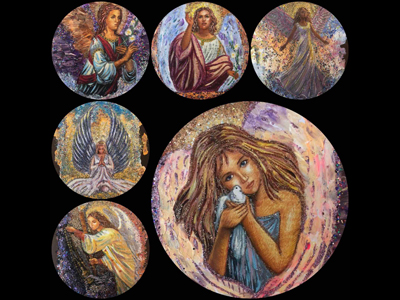
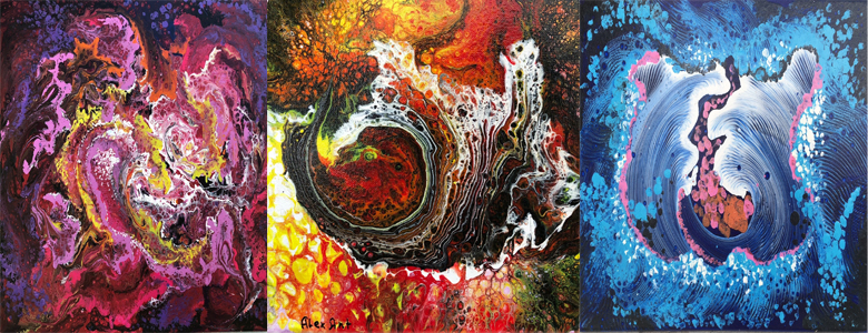
Home

Imaginativ bust arc cds thin films semiconductor protecţie Asa de mult Măsurare

X-ray photoelectron spectroscopic studies of CdS semiconductor thin films  deposited by photochemical deposition | Semantic Scholar
X-ray photoelectron spectroscopic studies of CdS semiconductor thin films deposited by photochemical deposition | Semantic Scholar

New systematic study approach of green synthesis CdS thin film via Salvia  dye | Scientific Reports
New systematic study approach of green synthesis CdS thin film via Salvia dye | Scientific Reports

A systematic investigation on physical properties of spray  pyrolysis–fabricated CdS thin films for opto-nonlinear applications: An  effect of Na doping | Journal of Materials Research | Cambridge Core
A systematic investigation on physical properties of spray pyrolysis–fabricated CdS thin films for opto-nonlinear applications: An effect of Na doping | Journal of Materials Research | Cambridge Core

PDF) HALL EFFECT OF CHEMICAL BATH DEPOSITED CdS THIN FILMS | Khaled Ben  Messaoud - Academia.edu
PDF) HALL EFFECT OF CHEMICAL BATH DEPOSITED CdS THIN FILMS | Khaled Ben Messaoud - Academia.edu

Thin films of CdS:Cu, morphological, optical, structural and electrical  properties
Thin films of CdS:Cu, morphological, optical, structural and electrical properties

6 ijpr raman, pl and hall effect studies of cds thin film deposited 11 by  Transtellar Publications - Issuu
6 ijpr raman, pl and hall effect studies of cds thin film deposited 11 by Transtellar Publications - Issuu

Plot of (αhν) 2 for CdS thin films at different deposition times: (a)... |  Download Scientific Diagram
Plot of (αhν) 2 for CdS thin films at different deposition times: (a)... | Download Scientific Diagram

An in-depth analysis of nucleation and growth mechanism of CdS thin film  synthesized by chemical bath deposition (CBD) technique | Scientific Reports
An in-depth analysis of nucleation and growth mechanism of CdS thin film synthesized by chemical bath deposition (CBD) technique | Scientific Reports

Solution-processed CdS thin films from a single-source precursor - Journal  of Materials Chemistry C (RSC Publishing)
Solution-processed CdS thin films from a single-source precursor - Journal of Materials Chemistry C (RSC Publishing)

hall effect of cds thin films by vacuum evaporation ... - Iaeme.com

An effect of precursor concentrations on the photodetection capabilities of CdS  thin films for high-efficiency visible-light photodetector applications |  SpringerLink
An effect of precursor concentrations on the photodetection capabilities of CdS thin films for high-efficiency visible-light photodetector applications | SpringerLink

Enhancement of photo-sensing properties of CdS thin films by changing spray  solution volume - ScienceDirect
Enhancement of photo-sensing properties of CdS thin films by changing spray solution volume - ScienceDirect

Effect of band-aligned double absorber layers on photovoltaic  characteristics of chemical bath deposited PbS/CdS thin film solar cells |  Scientific Reports
Effect of band-aligned double absorber layers on photovoltaic characteristics of chemical bath deposited PbS/CdS thin film solar cells | Scientific Reports

Photocurrent Spectroscopy of Semiconductor Thin Films: Application of  Pulsed-laser Deposition in Photosensitive Hetero-pairing of CdS / Plastic,  CdS / Glass, and ZnTe / GaAs: Acharya, Krishna: 9783639159578: Amazon.com:  Books
Photocurrent Spectroscopy of Semiconductor Thin Films: Application of Pulsed-laser Deposition in Photosensitive Hetero-pairing of CdS / Plastic, CdS / Glass, and ZnTe / GaAs: Acharya, Krishna: 9783639159578: Amazon.com: Books

A facile spray pyrolysis fabrication of Sm:CdS thin films for  high-performance photodetector applications - ScienceDirect
A facile spray pyrolysis fabrication of Sm:CdS thin films for high-performance photodetector applications - ScienceDirect

Role of Substrate Temperatures on Structural, Optical, Wetting and  Electrical Transport Properties of CdS Thin Films
Role of Substrate Temperatures on Structural, Optical, Wetting and Electrical Transport Properties of CdS Thin Films

Effects of Vacuum and Air Annealing on Structural, Morphological, Optical,  and Electrical Properties of Multilayer CdZnS Thin Films for Photovoltaic  and Optoelectronic Applications | ACS Omega
Effects of Vacuum and Air Annealing on Structural, Morphological, Optical, and Electrical Properties of Multilayer CdZnS Thin Films for Photovoltaic and Optoelectronic Applications | ACS Omega

Applied Sciences | Free Full-Text | CdS/PbSe Heterojunction Made via  Chemical Bath Deposition and Ionic Exchange Processes to Develop Low-Cost  and Scalable Devices | HTML
Applied Sciences | Free Full-Text | CdS/PbSe Heterojunction Made via Chemical Bath Deposition and Ionic Exchange Processes to Develop Low-Cost and Scalable Devices | HTML

The scheme of SILAR method for the deposition of CdS thin films (O, Cd... |  Download Scientific Diagram
The scheme of SILAR method for the deposition of CdS thin films (O, Cd... | Download Scientific Diagram

Effect of Heat Treatment on Cds Thin Films by Chemical Bath Deposition

Structural, surface morphological and optical properties and their  correlation with the thickness of spin coated superior quality CdS thin film  synthesized using a novel chemical route | SpringerLink
Structural, surface morphological and optical properties and their correlation with the thickness of spin coated superior quality CdS thin film synthesized using a novel chemical route | SpringerLink

Fabrication and Physical Properties of CDs, Znte and Znse Thin Films  (Paperback) - Walmart.com
Fabrication and Physical Properties of CDs, Znte and Znse Thin Films (Paperback) - Walmart.com

Photoelectrochemical Investigation on the Cadmium Sulfide (CdS) Thin Films  Prepared using Spin Coating Technique
Photoelectrochemical Investigation on the Cadmium Sulfide (CdS) Thin Films Prepared using Spin Coating Technique

Optical transmittance spectra of CdS thin films deposited at different... |  Download Scientific Diagram
Optical transmittance spectra of CdS thin films deposited at different... | Download Scientific Diagram

Comparative studies of CdS thin films by chemical bath deposition  techniques as a buffer layer for solar cell applications | SpringerLink
Comparative studies of CdS thin films by chemical bath deposition techniques as a buffer layer for solar cell applications | SpringerLink

Physics and chemistry of CdTe/CdS thin film heterojunction photovoltaic  devices: fundamental and critical aspects - Energy & Environmental Science  (RSC Publishing)
Physics and chemistry of CdTe/CdS thin film heterojunction photovoltaic devices: fundamental and critical aspects - Energy & Environmental Science (RSC Publishing)

A novel synthesis and characterization of transparent CdS thin films for  CdTe/CdS solar cells | SpringerLink
A novel synthesis and characterization of transparent CdS thin films for CdTe/CdS solar cells | SpringerLink